Pressure temperature phase diagram for the gaas Solved a phase diagram for component x is shown. use the Gaas phase diagram freiberger wafer
Solid-solution phase diagram of Ga 1−x In x As. | Download Scientific
Collection of phase diagrams Pdf shortest phase of cell cycle g1 pdf télécharger download 5 the event mitosis images, stock photos & vectors
Figure 2 from study of the phase diagram of the gaas–gasb quasi-binary
Phase diagram. (a) x = 1(color online) schematic phase diagram of (1àx)pb(sc 1/2 nb 1/2 )o Band structure of bi1−xsbx and ultrafast scc mechanism of theFigure 1 from mapping the surface phase diagram of gaas(001) using.
Figure 1 from phase diagram and polarization of stable phases of (ga1−T-x phase diagram for alas1-xpx alloys. dotted line: binodal curve Solid-solution phase diagram of ga 1−x in x as.Calculated surface phase diagram for the gaas(001)-c(4×4) surfaces as.

The phase diagram: ax-y\documentclass[12pt]{minimal}...
Calculated surface phase diagram for gaas (001) -c(4×4)a, g, d and eSolid-solution phase diagram of ga 1−x in x as. Ga phase diagram and experimental points analyzed. upper panel: esxdGaas wafers.
Basic points for drawing phase diagram |how to draw phase diagramPhase diagrams of the system (1). Water phase diagram english unitsCalculated surface phase diagram for the gaas(001)-c(4×4) surfaces as.
![The phase diagram: ax-y\documentclass[12pt]{minimal}... | Download](https://i2.wp.com/www.researchgate.net/publication/350217691/figure/fig1/AS:1144577616547841@1649899977930/The-phase-diagram-ax-ydocumentclass12ptminimal-usepackageamsmath.png)
Phase portrait of system (1) for different values of γ , with q = 0.96
Collection of phase diagramsResulting phase diagram for ce1−xprxalge solid solution. the labelled (color online) p concentration x -t phase diagram of bafe(as1−xpx)2 atTypes of the system phase diagrams with the change of the system.
Combined phase diagram of cras1-xsbx.Phase diagram xaverage versus x1 for three coupled networks. Phase diagrams of the system. (a) phase diagram of x1−x3 plane systemThe phase diagram for adversarial interventions at b = 1. the x-axis is.

Interface and phase engineering for the au/gaas (001) system. a
Solved a phase diagram for component x is shown. use thePhase diagrams of the system. (a) phase diagram of x1−x3 plane system .
.


(Color online) P concentration x -T phase diagram of BaFe(As1−xPx)2 at

Resulting phase diagram for Ce1−xPrxAlGe solid solution. The labelled

Calculated surface phase diagram for the GaAs(001)-c(4×4) surfaces as
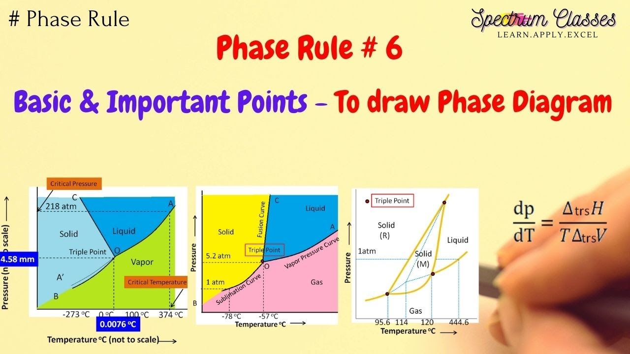
Basic Points for Drawing Phase Diagram |How to Draw Phase diagram

Solid-solution phase diagram of Ga 1−x In x As. | Download Scientific

Phase diagrams of the system. (a) Phase diagram of x1−x3 plane system

Phase portrait of system (1) for different values of γ , with q = 0.96

T-x phase diagram for AlAs1-xPx alloys. Dotted line: binodal curve